


FSP-Patented MIA IC™ Cuts Costs and Reduces Energy Consumption in New Efficient Switching-Mode Power Supply
MIA IC™ Whitepaper
Overviews
- Introduction
- Background
- FSP MIA IC™ 6600 Features
- FSP MIA IC™ 6601 Features
- Why MIA IC
- Benefits of Implementing FSP MIA IC
- Implement an Optimized Power Source to Minimize Cost and Environmental Issues
- New Technology
- A Powerful Multiplier Divider
- Method for Controlling the Startup Cycle and Circuit
- Variable-Frequency Circuit with a Compensation Mechanism
- Abnormal Power Protection
- Cycle Modulation Circuit Capable of Limiting Peak Voltage
- Self-Excitation Synchronous Rectification Driver
- Chop Wave Control Circuit
- Post Regulation Control Circuit
- Conclusion
- Reference
Introduction
In an era where everything is becoming smaller and smaller, the need to compress everything comes at a cost. We are also moving into a societal culture where manufacturers are becoming aware that the devices they build plays a vital role with the outcome of the environment. More and more challenges come along in which we try to produce products that are environmentally-friendly and pushes the boundaries of new tech. To that end we have to look deeper into how we facilitate power and make use of it.
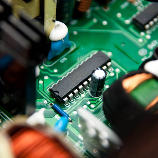
The FSP MIA IC™ chipset features a reliable and efficient operational current to power supply ratio. The result is increased power density and simpler designs for PC manufacturers, helping them accelerate time to market and realize higher revenues. This white paper covers advantages, functions and technical details of the FSP MIA IC™. Product miniaturization puts extra pressure on designers to scale down the power system. Efficient usage demands that newer equipment accept higher-voltage inputs near the point of usage.
Background
Through years of research and development, the original patented MIA IC™ (Multiple Intelligence Ability) technology chipset was unveiled. The combination of Active-clamp topology and an MIA IC™ is the perfect solution for a stable, eco-friendly and long–life Power Supply Unit. FSP and the R&D Team are always striving for better quality and create green, cost savings innovations for you.
FSP MIA IC™ 6600 Features
- 12 Patents
- Provides
- PFC
- PWM
- Stand-by three stages controls and synchronizing Function in one device
- Low operation current (1.5mA typ)
- Active Clamp structure with low loss operation
FSP MIA IC™ 6601 Features
- 9 Patents
- Provides synchronous and post regulation control functionality in one device
- High efficiency post regulation
- Over current protection
Why MIA IC
MIA IC™ Technology (Multiple Intelligence Ability) is the very first IC chipset with a unique multi-functional combination – PWM, ZCS PFC, Post SR, Active Clamp, Double-circuited OVP that provides ultimate performance & the highest protection to your system. This new innovation makes power supplies compact in size, high in efficiency, and adds maximum protection (OVP, UVP, OCP, SCP, OPP).
Benefits of Implementing FSP MIA IC™
With the implementation of FSP’s own patented MIA IC™ Technology, two major breakthroughs have been achieved on the PSU design. First, by implementing our patented control IC plus the mature Active Clamp topology, we are able to realize Zero Current Switching and thus efficiency was improved tremendously on AC-DC power conversions. Therefore, less energy is converted and less heat expended. Most important of all, higher efficiency provides you the benefit of saving you money on your electricity bill.
Moreover, PFC, PWM, Stand-by, and Synchronous rectifying are integrated within MIA IC™ Technology and its supporting circuitries. A smaller component count was made possible. And this fact contributes greatly to reduce air resistance within a PSU. Airflow through components has never been more efficient. The technology which makes the MIA IC™ chipset so impressive is the AT Clamp’s ability to reduce overall parts and material costs for other components and the high efficiency with which it is able to transmit power. The very design structure enables a higher cost per power value in PSU. This is ideal for applying it in industries like the automotive and industrial sphere. It can also save power sources when developing IoT, networking, and storage devices. Because these units have small power footprints, the goal is to create ever cost saving devises that will power these new technologies.
Implement an Optimized Power Source to Minimize Cost and Environmental Issues
High-voltage innovations are making the transmission and conversion of electrical power more efficient, so less power is lost between the source and the end equipment. These innovations complement changes in electricity and voltage power. It also lowers the operational current, controls synchronous and post regulation functions in one device, and offers higher efficiency in post regulation.
FSP’s MIA (Multiple Intelligence Ability) IC technology is the first manufacturer to offer multi-functionality - PWM, ZCS, Post SR, and Active Clamping. Dual-circuit Over Voltage Protection (OVP) provides ultimate performance and protection to the system. Improvements in chipset design reduces power supply sizes making them more attractive to overall PC construction. The underlying technology is to control the startup cycle of an integrated circuit in a circuit system. The method and circuit determines whether or not an input power and a bias voltage power has reached a normal operating voltage range to control the bias voltage power to produce a startup cycle of the integrated circuit.
New Technology
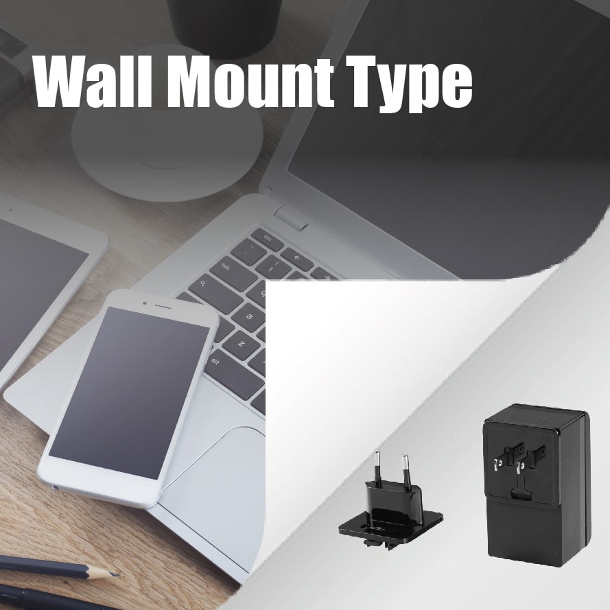
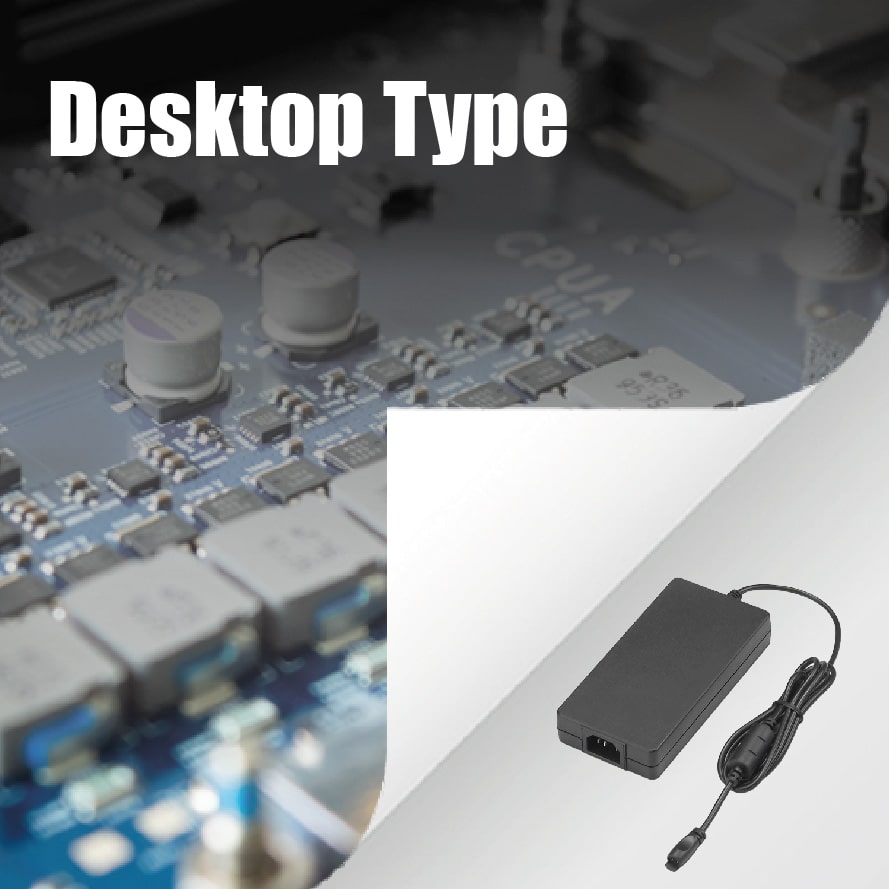
FSP incorporates their technology head on by utilizing the MIA chipset into their PC PSU. This has been incorporated into their FSP250-60SGV, and FSP300-60SGV. The FSP250-60SGV features a 250W power supply, +5V stand by, a second 12V rail and remote ON/OFF control and “Power factor collector (PFC)” circuit to meet EPA requirement of input range with in 115V/60HZ & 230V/50Hz. The FSP300-60SGV holds similar features but has more wattage at 300W. The immediate cost saving and power throughput helps to define this technology as a necessity to helping control power within the system.
The MIA IC™ Patented Chip using 3 years to develop, what is the feature and advantage?
MIA IC™(Multiple-Intelligence Ability) use Active-clamp circuit, and combine with PWM, ZCS PFC, Post SR, Double-circuited OVP. Make the PSU smaller but higher efficiency, stable and includes many protections (OVP,UVP,OCP,SCP,OPP).
- ZCS PFC (power factor correction→ZCS): Normal PFC is high switching loss and have EMI interference issues. ZCS PFC helps to reduce this issue.
- Post SR (Post synchronous rectifier) does the same as the DC to DC converter. DC to DC switches lower to the 12V out to 3.3V 5V, which is low efficiency compared to the Post SR
- Active Clamp topology - A power supply circuit is the basic structure similar to the double-crystal architecture (dual switch forward topology), also known as active-clamp architecture
- Double circuited OVP - This is known as overvoltage protection (OVP) used at the output to ensure the safety of a motherboard, but ignores the primary side there is a danger of large electrolytic capacitors (Bulk cap) existing, but a boost circuit (PFC) capacitor exception will cause an explosion . Double circuited OVP is an additional overvoltage protection (OVP) which ensures that the capacitor (Bulk cap) Security is exhaustive
- Active Clamp topology - A power supply circuit is the basic structure,it is called active clamp architecture. It's like SRC, LLC, Forward, Fly-back - the architecture is used in a wide range of power supplies.
- Active clamp Advantages: 1. Zero-voltage switching mode (ZVS) used to reduce switching losses 、 2. Wide operating cycle (DUTY) function, can reduce the magnetic loss
Zero current switching (ZCS) - In order to avoid exchange losses (Switching loss), it will normally switch element (MOSFET) operating at zero current switching or zero voltage switching state. Zero current switching (ZCS) is called zero-current switching mode, as the name suggests is that when the switching element is started (turn on) the conduction current is zero.
A Powerful Multiplier Divider
Multiplier dividers are widely used on modern electronic devices. They aim to generate an output signal proportional to two or more input signals. The output signal may be voltage or current. One of the common applications of the multiplier divider is on a PFC circuit to generate a control signal through an input current, a feedback signal, and an input voltage.
These days safety regulations and power saving requirements are increasingly strict. Hence power supplies are usually equipped with a PFC circuit to reduce resonance waves and regulate current phases to improve power utilization efficiency. The conventional passive PFC circuit can improve its efficiency only about 70%, while an active PFC circuit can improve its power utilization efficiency above 80%. Hence, active PFC circuits are becoming a necessary element for almost all types of power supplies.
The MIA IC™ chipset includes a buffer, a resistor, three sets of differential converters, two dividers, two multipliers, and a pulse generator. Each multiplier has a peak detector and a voltage integrator with the time period controlled by the divider. Each divider has two waveform generators, which form independent dividers, and have the structure passing through the multipliers at a next stage through the period. And the pulse generator has two bar gate units and a square wave generator to isolate waveform and reset the bar gate units.
Method for Controlling the Startup Cycle and Circuit
The method and circuit determine whether or not an input power of the circuit system and a bias voltage power of the integrated circuit have reached a normal operating voltage range. This method and circuit controls the bias voltage power to produce a start-up cycle of the integrated circuit. The method and circuit also provide a protection mechanism for an overload of the circuit system overload, so that the integrated circuit can moderate surges and prevent damages.
In general, a power supply includes a power factor correction (PFC) unit and a pulse wave control unit, or further includes a stationary power control unit. All of the units are integrated into several different integrated circuits (ICs) or into a single integrated circuit in order to save space and power loss. Furthermore, a detection input voltage and a self-start function can be added to the integrated circuit, so that the integrated circuit can control bias voltage power (Vcc) by detecting and determining whether or not the inputted alternating current of the integrated circuit has reached the operating voltage, and then the integrated circuit decides whether or not to start a circuit unit in the integrated circuit. If the inputted alternating current has not reached a normal operating voltage, the integrated circuit will shut down automatically and continually detect whether or not the alternating current falls within the range of the normal operating voltage.
To prevent overloading, overheating, and power loss, the MIA IC™ chipset is equipped with a method to manage the start-up cycle of an integrated circuit. The MIA IC™ sets a start-up voltage value for starting the integrated circuit, and a cut-off voltage value for shutting down the integrated circuit. Furthermore, the integrated circuit obtains bias voltage power when an AC voltage is inputted into the circuit system, and the start-up cycle rises from idle voltage value to start-up voltage value through bias voltage power to start the integrated circuit or drops from the start-up voltage value to the cut-off voltage value to shut down the integrated circuit.
The method includes steps for defining a normal operating voltage value and the idle voltage value and determining whether or not the input power average has reached the normal operating voltage value, and maintaining the bias voltage power at the idle voltage value or increasing the bias voltage power to the start-up voltage value for issuing an instruction of starting the integrated circuit after the determination. The method also includes steps to drop the bias voltage power to idle voltage and then to raise it to start-up voltage value when the system is overloaded in order to avoid a sudden change of voltage that may damage the integrated circuit.
Variable-Frequency Circuit with a Compensation Mechanism
Environmental protection regulations have become stricter and stricter all over the world, and electric appliances also have high standards for power consumption. Therefore, a power supply usually has an energy-saving circuit to control the output mode when the load varies. This energy-saving circuit reduces circuit-switching loss to the minimum.
A conventional power supply comprises: a primary side rectifier unit, a transformer, a PWM (Pulse Width Modulation) unit, a switch unit, and a feedback unit. The feedback unit is coupled to the secondary side and further comprises: a current feedback unit and a voltage feedback unit. The primary-side rectifier unit receives external power and performs a preliminary conversion and then transfers power to the transformer.
The transformer converts power from the primary side to the secondary side. Then, the power is rectified into a stable DC output. The PWM unit provides a working cycle signal to control the switch unit to determine whether to turn on or turn off the primary side of the transformer. The PWM unit can adjust the duty cycle ratio of the working cycle signal according to the feedback signal provided by the current feedback unit and the voltage feedback unit. However, the adjustment of duty cycle ratio has its limits. Therefore, the industry developed a variable-frequency energy-saving circuit and a cycle-skipping energy-saving circuit. However, the cycle modification in a variable-frequency or cycle-skipping energy-saving circuit usually causes voltage variation.
Abnormal Power Protection
The MIA IC™ chipset’s abnormal power protection circuit includes a power detection unit, a voltage drop correction unit, a drop out detection unit, a delay unit and a delay-masking unit. This circuit detects brown-out conditions and power drop-off conditions. The power supply includes a power factor correction unit, which has an output capacitor. When a power abnormal condition occurs all units of the power supply can be set off sequentially according to a delay time to protect circuit elements and a connecting computer.
A power supply receives AC power and converts it to steady DC power for computer operation. The general electric power users occasionally encounter blackout or brownout conditions. Hence, most power supplies provide features that guard against abnormal voltage. Abnormal AC power conditions occurring in general houses mainly can be divided into two types: one is a drop out in which the voltage drops significantly and instantly from a normal value. The duration can be very short, but the voltage is excessively low or at a lower level constantly, thus the power becomes unusable. This can be caused by damaged electrical equipment or by abrupt starts great power loads at the user end (such as a motor of a great capacity being started suddenly). The MIA IC™ provides an abnormal power protection circuit to control the OFF time series of a power supply when an abnormal voltage occurs. The power supply includes a rectification unit, a power factor correction unit, a transformer, a main power output unit and a standby power output unit. It also includes a power factor correction control unit, a pulse width modulation (PWM) unit, a standby power control unit and the power abnormal protection circuit.
The power abnormal protection circuit includes a power detection unit, a voltage drop correction unit, a drop out detection unit, a delay unit and a delay-masking unit to detect the average value of input power of the power supply to determine whether a brown out condition occurs. It also detects the voltage of an output capacitor in the power factor correction unit to determine whether a drop out condition occurs.
Cycle Modulation Circuit Capable of Limiting Peak Voltage
The MIA IC™ ha a cycle modulation circuit capable of limiting peak voltage. It provides a pulse width control signal to a rear end power-driving unit including a comparison unit, an input voltage source and a linear voltage generation unit. The comparison unit compares an oscillation waveform signal generated by the linear voltage generation unit against a base value of a waveform signal level generated by the input voltage source to modulate and output the pulse width control signal of a combined cycle consisting of a high level and a low level. The pulse width control signal is input to the rear power-driving unit to limit the power-driving unit in an equally restricted voltage peak value zone and determines the allowable duty cycle according to the level waveform signal.
Power supply is an indispensable element on many information products. Its most important mission is to provide sufficient and stable voltage. Otherwise equipment cannot be started normally, and unpredictable voltage and current surges can cause damage of equipment.
The primary objective of the MIA IC™ chipset is to provide a cycle modulation circuit to limit the maximum duty cycle of a PWM circuit to stabilize the peak-to-peak value of the driving voltage. The cycle modulation circuit mainly includes a comparison unit, an input voltage source and a linear voltage generation unit.
The comparison unit has a signal input end and a signal output end. The comparison unit uses a waveform signal level generated by an input voltage source as a base value to perform level comparison with an oscillation waveform signal produced by a linear voltage generation unit, then modulates and outputs a pulse width control signal which has a combined cycle consisting of a high level and a low level. The pulse width control signal is input to a rear end power-driving unit that includes the PWM circuit, thereby to limit the power-driving unit in an equally restricted voltage peak value zone and determine the allowable duty cycle according to the waveform signal level.
Self-Excitation Synchronous Rectification Driver
The MIA IC™ chipset offers a self-excitation synchronous rectification driver, which comprises a self-excitation coil, a self-excitation driver, a synchronous-signal source, a pulse transformer, a positive/negative edge detector, and a latch unit. The synchronous-signal source generates a synchronous signal to attain an external synchronous function. When the frequency is abnormal, the first and second rectifier switches of the rectification unit on the power supply are forced to turn on or turn off. Thereby, the first and second rectifier switches can turn on alternately, and the first and second rectifier switches are limited to within the highest and lowest working frequencies during the zero-load stage or the shutdown stage. Thus, the frequency of the synchronous rectification driver is under control, and abnormal voltage will not occur.
The MIA IC™ chipset provides a self-excitation rectification driver, particularly to a rectification driver, which utilizes synchronous signals to make two rectifier switches turn on alternately and limit the working frequencies thereof.
A power supply usually comprises a main power system and a standby power system. By a main transformer, the main power system is divided into a power driver unit at the primary side and a rectification unit at the secondary side. The rear end of the rectification unit is coupled to a voltage feedback unit to correct the working period of the power driver unit. In a conventional power supply unit, the power driver unit has a primary driver unit SW1, a secondary driver unit SW2 and a main transformer TX.1. The rectification unit utilizes a self-excitation coil Lo to generate a self-excitation phenomenon. The charge/ discharge of the self-excitation coil Lo is used to control the turn-on of a first rectifier switch and a second rectifier switch.
Self-excitation synchronous rectification technologies have been widely used in forward-type power transformation devices. The sensed voltage of the main transformer is directly or indirectly used to drive the synchronous rectifier switch elements and achieve synchronous self-excitation in all the existing patents of self-excitation synchronous rectification technologies.
The MIA IC™ chipset provides a self-excitation rectification driver with an external synchronous function, wherein during zero-load or underload-shutdown stage, an external synchronous signal regulates the self-excitation frequency to be within a normal working range lest the circuit be damaged by abnormal voltage.
Chop Wave Control Circuit
A chop-wave circuit can be seen as a switch circuit with a truncated waveform. It is widely used on a forward transformation circuit that includes a power driving unit, a transformer, a main output unit and at least one auxiliary output unit. The power-driving unit delivers electric power through the transformer to the main output unit and auxiliary output unit. The main output unit generates a first sync signal and a second sync signal through a self-excited driving unit to control respectively a main output switch and a main flywheel switch that are ON alternately to deliver output.
The chop-wave circuit is used on the secondary side of a transformer to control the level of auxiliary output voltage through turning ON/OFF the switches. The chop-wave circuit to control the auxiliary output circuit is controlled by a comparator A. The comparator A has one end capturing the voltage of the secondary side of the transformer 2 (T2) and another end capturing a feedback voltage from an output end of the auxiliary output circuit to the other end. These two are compared by the comparator A, then an output is generated to control the ON/OFF switch element to alter the electric power output by the auxiliary output circuit.
As the comparator has a significant inherent transfer delay, transient action is slow and the response is not desirable. Moreover, the comparator does not have a latchup function. Hence, in the event that noise interference occurs to one or two input signals at the two ends of the comparator after weighed and balanced erroneous actions are prone to take place and result in control cycle fluctuation. Hence it is relatively not stable.
The chop-wave control circuit is adopted to be used on a forward transformation circuit, which includes a power-driving unit, a transformer, a main output unit, and at least one auxiliary output unit. The auxiliary output unit includes an auxiliary output switch and an auxiliary flywheel switch and a chop-wave switch that are controlled by the chop-wave control circuit.
Post Regulation Control Circuit
A power supply that provides multiple outputs of different potentials is a technique known in the art. Commonly seen power supplies usually have a transformer with a secondary side divided into at least one primary output circuit and a post regulation circuit connecting to the primary output circuit. The primary output circuit aims to provide primary output power, which forms a greater proportion of output power through winding induction on the secondary side of the transformer.
The post regulation circuit provides ancillary output power with a lower voltage and lower power by lowering the voltage of the primary output power. Take the power supply of a general desktop computer as an example, the primary output power with power and current at a greater proportion of the total output is 12V and 5V, and is delivered through two windings. The post regulation circuit is then employed to generate 3.3V.
The MIA IC™ chipset provides a post regulation control circuit to control ancillary output power generated by a power supply. The power supply includes a transformer which has a secondary side connected to at least one primary output circuit. The MIA IC™ includes a post regulation circuit connected to the primary output circuit and receives a primary output power from the primary output circuit. The post regulation circuit comprises a set of switch unit to regulate the primary output power to an ancillary output power and a monitor circuit to control duty time series of the switch unit.
Conclusion
The MIA IC™ ha a cycle modulation circuit capable of limiting peak voltage. It provides a pulse width control signal to a rear end power-driving unit including a comparison unit, an input voltage source and a linear voltage generation unit. The comparison unit compares an oscillation waveform signal generated by the linear voltage generation unit against a base value of a waveform signal level generated by the input voltage source to modulate and output the pulse width control signal of a combined cycle consisting of a high level and a low level. The pulse width control signal is input to the rear power-driving unit to limit the power-driving unit in an equally restricted voltage peak value zone and determines the allowable duty cycle according to the level waveform signal.
Power supply is an indispensable element on many information products. Its most important mission is to provide sufficient and stable voltage. Otherwise equipment cannot be started normally, and unpredictable voltage and current surges can cause damage of equipment.
Reference
United States Patent and Trademark Office
| US Patent No. | |
| US2008/0304195 A1 | Power abnormal protection circuit |
| US2008/0222230 A1 | Multiplier-divider having error offset function |
| US2009/0028273 A1 | Variable-frequency circuit with a compensation mechanism |
| US2008/0310196 A1 | Circuit and method for controlling the start-up cycle of a power supply |
| US2008/0111602 A1 | Cycle modulation circuit capable of limiting peak voltage |
| US2008/0192517 A1 | Self-excitation synchronous rectification driver |
| US7,391,626 B1 | Chop wave control circuit |
| US2001/0156481 A1 | Post Regulation With Leading-Edge Over Current Controller |
R&D Status and Result
FSP (Taiwan stock number3015) founded 1993, is one of the leading PSU manufacturers in the world. With more than 400members in its R&D team to cover all kinds of PSU needs, such as PC PSU, IPC PSU, Medical PSU, LCD TV PSU, SSL, Adapters, UPS, Industrial PSU, Energy Storage System, PV Inverter, Retail, and much more.
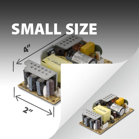
FSP's total solution can reduce 50% of the components and reduce 20% of the weight compared to traditional electric circuit. FSP has several outstanding products: a server PSU which create the power density of 50.7W/in³, a slim adaptor that’s less than 16.5mm. FSP won the prestigious ASIC IC design / module ability for its MIA IC™ patented chipset, which has achieved greater than 93% energy efficiency.
For more FSP product information, please visit:
About FSP:
Founded in 1993 and one of the leading supplier of power supply products in the world, FSP Group (3015: Taiwan) meets varied user demands in power supplies with its 400-person strong R&D team, robust production capacity and comprehensive production lines. With more than 422 models certified to 80 PLUS standards, the world number one in 80 PLUS certification, enables users to enjoy Eco-friendly technologies by providing the best environment protection and quality power supply products.
Related Articles


About FSP
FSP Group is one of the global leading power supply manufacturer. Since 1993, FSP Group has followed the management conception “service, profession, and innovation” to fulfill its responsibilities as a green energy resolution supplier.